Zero Humans in the Loop: Inside Frostbite, the CPU That AI Discovered, Designed, and Verified — Claiming 4.59× the Performance per Watt


Zero Humans in the Loop: Inside Frostbite, the CPU That AI Discovered, Designed, and Verified — Claiming 4.59× the Performance per Watt
Published: November 20, 2026 | Reading Time: ~10 minutes | Channel: techminute
TL;DR: Architect Labs' Frostbite is a general-purpose CPU with a brand-new instruction set — discovered, designed, verified, and taken to final chip layout end-to-end by AI agent swarms — claiming 4.59× the performance per watt and 8.77× the performance per area of a modern dual-issue in-order core across 25 workloads, all before a single transistor has been fabbed.
Architect Labs says its AI systems have built a new general-purpose CPU from scratch — instruction set, microarchitecture, RTL, verification, and final GDS layout — with no human architect in the design loop. The result, called Frostbite, is built on a 36-year-old mathematical model of computation called interaction nets, and the company reports a geometric mean of 4.59× performance per watt versus a modern, silicon-proven dual-issue in-order core across 25 workloads, 15 of which were held out until final evaluation. The announcement hit the top of Hacker News this morning (352 points and 228 comments as of this writing), and the numbers — if they survive contact with real silicon — would be the largest single-step CPU efficiency jump in decades. But every result is pre-silicon simulation, the baseline chip's identity is undisclosed "for legal reasons," and the comparator is an efficiency-focused in-order core, not a desktop-class out-of-order monster. Here's what's actually inside the claim, and what the machines did to keep each other honest along the way.
Key Takeaways
- Frostbite is a complete, general-purpose CPU architecture with a new ISA — the AI iterated across compiler, ISA, architecture, microarchitecture, RTL, verification, and final GDS with "zero architectural priors," per the official Architect Labs post.
- Headline results (all pre-silicon, 7nm synthesis/layout): 4.59× perf/W geomean over 25 workloads (6.02× on the 10 tuning workloads, 3.83× on the 15 held-out), plus 8.77× perf/area — synthesized at 800 MHz, 500 MHz in final layout.
- The verification story may matter more than the benchmark: specs live in ASL, an in-house formal language that lowered to 800,000+ lines of Lean proofs — a machine-checkable "single source of truth" the company credits with preventing agent "reward-hacking."
- The swarm's process had real hygiene: a 141-page architecture PDF was deleted after the first RTL generation proved its estimates "well off what was physically possible," and the final model agreed with physically synthesized RTL within 1–5%.
- Caveats are substantial: no manufactured chip, no tapeout date, the comparison CPU is undisclosed and in-order, workloads were company-selected, and industry-standard SPEC/PARSEC comparisons are only promised for the future.
The Context: Why CPU Design Needed a Shove
Single-core CPU performance has been on a plateau since the early 2000s, and Architect Labs' diagnosis of why is refreshingly blunt. Mainstream languages hide dependencies: any compiled program may read or write any variable through shared, mutable state, so "modern CPU hardware assumes the worst case and rediscovers, at runtime, which instructions actually depend on each other." The industry's answer has been to go wide — the big multicore Xeon, Zen, and NVIDIA Vera parts — but scaling cores means maintaining "the illusion that every core sees the same memory," and that illusion is expensive. Deep cache hierarchies and coherence protocols burn area and power, and scale poorly.
That's the tax Frostbite tries to abolish. The broader context: this is the second act for Architect Labs (the company is registered as Architect Silicon Inc., per its site footer). Its previous post, Redwood, showed that given an architecture, its AI systems could implement, verify, and deploy an inference accelerator in record time. Frostbite asks a harder question — the one every lab in the AI-chip stack is now circling: could AI systems, given freedom and guardrails, make a novel hardware discovery that beats human designs outright?
It's the same gravity that pulled OpenAI and Synopsys into building GPT-Synopsys for chip design flows, and it's why this story hit #1 on Hacker News within hours. Everyone is asking whether the architect is becoming a prompt.
Under the Hood: Interaction Nets, Finally Asked to Do Something
The mathematical core of Frostbite isn't new. Interaction nets were introduced by Yves Lafont in 1990. A program is a graph of nodes; computation happens by rewriting pairs of nodes connected through their ports. Three properties do all the work:
- Every rewrite is local — it only touches a small neighborhood of the graph.
- Every node has exactly one principal port — so no two "active pairs" ever overlap, meaning rewrites can run in any order, or all at once, and the result is identical.
- Every value has exactly one owner — the model is linear, so there's no shared mutable state for hardware to guard.
That third property is the killer. No shared mutable state means no cache coherence problem, because there's nothing to keep coherent. Parallelism isn't extracted at runtime by out-of-order machinery; it falls straight out of the program's graph.
Architect Labs' favorite illustration is the five-queens puzzle on a five-by-five board. A C++ program walks the search tree one candidate at a time. The same search as an interaction net exposes 3,183 interactions with a critical path of only 262 steps — on average, about 12 interactions are ready to run at every step. Nothing about the program was rewritten to get that parallelism; the dependencies were simply never thrown away.
Programs are written in Vine, a language with Rust-like syntax (per Notebookcheck's coverage), compiled to an intermediate representation called Ivy, whose optimizer reduces the graph to exactly three primitives: data, computation, and control nodes (per LavX News).
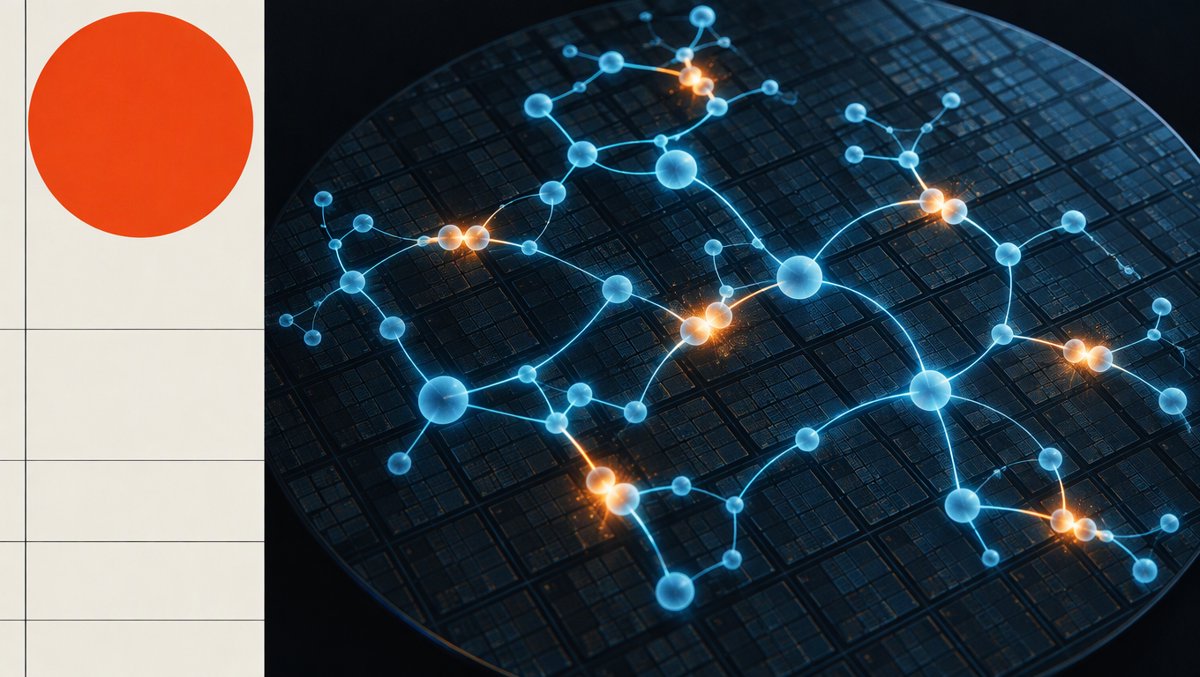
Physically, Frostbite isn't one big core — it's a grid of small computing tiles, each with its own local memory, arranged on a 7nm layout as a 4×4 tile grid with L3 nodes at the edges. Each tile runs its own work first and picks up neighbors' slack when idle; if there's nothing to do, it powers down. There is no central scheduler anywhere in the picture.
How the Machines Kept Each Other Honest
The benchmark numbers are the hook, but the process is the story — because unleashing swarms of LLM-driven agents on a silicon program is exactly how you get confident, well-formatted garbage. Architect Labs' answer is a verification regime most human chip teams don't run:
Formal contracts instead of English PDFs. The company built ASL, an in-house specification language with "machine-checkable translations and refinements" between RTL, system models, UVM, and SystemVerilog assertions. ASL translates natively to Lean, the theorem prover, and Frostbite's specification ultimately lowered to more than 800,000 lines of Lean. The company's rationale is worth quoting: natural language "cannot capture every detail an implementation needs precisely and unambiguously, and it cannot guarantee that every agent hallucination is caught." In a world where the AI writes the spec, the spec has to be provable. The ASL contract was the single source of truth for the whole program — and per the company, having "a single, provable source of truth prevents a large class of bugs, silly mistakes, and reward-hacking instances when deploying large agent swarms."
The PDF that got deleted. Early in the program, agents synthesized research papers and benchmarks, built Python trade-off models, and produced a 141-page architecture document. After the first RTL generation, the humans checked it and deleted it — many of its estimates were "well off what was physically possible." The lesson baked into the process: models that haven't touched synthesis are fiction.
The 250% recalibration. The chip's system model, Arcmodel, initially disagreed with timing-converged RTL by up to 250% in the worst case on power. An autonomous pipeline then traced RTL power hotspots down to formal-spec counters (SRAM reads/writes, operation counts, flits, credit returns), searched over Python predictor functions, and iterated until model and silicon agreed within 5%. Post-alignment, Arcmodel runs 660× faster than RTL simulation, which let the swarm do cross-stack optimizations — like inventing fine-grained clock-gating tricks and adjusting the software runtime to match — "in a matter of hours." In a traditional ASIC flow, that loop takes quarters, not hours.
Selection pressure that actually selected. Across four architecture searches plus a final round of ablations, agent swarms proposed 58 ideas and kept 37 — everything from clock gates on a running tile to smaller L3 tables. Ideas were checked against contracts, modeled, implemented in RTL, measured for power, and kept or dropped on the evidence.
If you've been following the agent-safety conversation all year, the pattern here will look familiar: don't trust the model, trust the machine-checkable thing the model must satisfy. Architect Labs just applied that doctrine to silicon.
By the Numbers: The Benchmarks, With Footnotes
| Metric | Baseline (TCPU) | Frostbite | Improvement |
|---|---|---|---|
| Performance per watt (geomean, 25 workloads) | 1.0× | 4.59× | +359% |
| Perf/W — 10 tuning workloads | 1.0× | 6.02× | +502% |
| Perf/W — 15 held-out workloads | 1.0× | 3.83× | +283% |
| Performance per area | 1.0× (0.895 mm²) | 8.77× (0.792 mm²) | +777% |
| Synthesis frequency | — | 800 MHz | — |
| Final layout frequency | — | 500 MHz | — |
The held-out number is the one to take seriously: 3.83× on workloads the swarm never tuned against is a genuinely good generalization result, and the company's decision to hold out 15 of 25 workloads — including five practical ones added later (a Kalman filter, PCA, finite element analysis, an LU solve, and LZ4 decompression) — is better benchmark hygiene than a lot of published accelerator papers manage. Workloads ranged from dense parallel kernels (GEMM, conv2d, FFT, radix sort — the latter three following SPLASH-2 implementations at 64× smaller scale, since full sizes are unsuitable for exploration) to nasty irregular code: JSON parsing, Huffman coding, k-d trees, recursive Fibonacci. Frostbite is strongest on parallel work but, per the company, still beats the baseline on branching and dynamic code.
The energy breakdown tells you where the win comes from:
| Energy destination | TCPU | Frostbite quad |
|---|---|---|
| Clock distribution | 49% | 41% |
| Memory (of non-clock energy) | 57% | 38% |
| Fetch/decode/issue (of non-clock) | 27% | 6% |
| On-chip network + scheduler | — | 26% |
The conventional core burns over a quarter of its useful energy fetching, decoding, and issuing instructions — the entire x86-era overhead of pretending programs are instruction streams. Frostbite cuts that to 6%. That's the interaction-net dividend: when the graph is the program, there's no decode tax to pay.
Two footnotes belong under that table, in bold. First, the baseline — "TCPU," a "modern, silicon-proven superscalar (dual-issue, in-order) CPU core" — is not identified; the company declined to name it "for legal reasons." An in-order dual-issue core is a fair efficiency comparator (think embedded-class designs), but it is not an Apple M-series or Zen 6 big core. Second, every number above is pre-silicon: synthesis, layout, and correlated modeling — impressive, correlated modeling, but modeling. Notebookcheck states it plainly: "the results come from pre-silicon simulations rather than a physical processor."
The Part Nobody Programmed: Emergent Work Stealing
The detail that should make actual CPU architects sit up: the agents reinvented one of parallel computing's classic scheduling problems — work stealing — as a hardware protocol, with no human specifying it. Because parallelism is spread across space rather than managed by a scheduler, the design converged on three rules:
- A tile runs its own work first, from its input ports.
- If empty, it takes work from a neighboring tile with spare work.
- If none is found, it goes inactive to save power.
Around that, the compiler and hardware grew a full continuation mechanism: loops or branches that split into parallel pieces of unknown size park their continuation in a frame manager record in local memory, drop tasks onto a hardware work queue, and as tasks finish anywhere on the chip — in any order — return packets decrement the parked record's counter and wake the next section "the instant the last piece arrives." Architect Labs says this behavior "can be traced to necessity on specific regressions and hill-climbing performance metrics" — in other words, it wasn't designed, it was selected. The company's ISA also grew expected features (wide bundles, hardware loop counters, streams) alongside stranger ones: dynamic take/peek/copy operations that let tiles pull values from other parts of the net running in parallel.
What This Changes
If the claim holds at all, the implications stack up fast:
For chips: Architect Labs' stated thesis is that every class of silicon — datacenter CPUs, AI accelerators, networking switches, NICs — will "go through similar fundamental architectural shifts" as AI design systems mature. The company's roadmap is unusually open for a chip startup: release the RTL and ISA, build an FPGA-based software playground, develop a preliminary OS, and benchmark larger Frostbite configurations against real multicore CPUs on SPEC and PARSEC. If the RTL and ISA actually ship, this becomes the most auditable "AI-designed hardware" claim anyone has made.
For the industry's adoption path: the sharpest community take came from Hacker News commenter mike_hearn, who argued Frostbite doesn't need to obsolete x86 to succeed: "You can just add extra accelerator chips. GPUs did this, NPUs are trying to do this... If this stuff works, it'll surface first as some PCIe extension device that work can be dispatched to when it makes sense." That's almost certainly right — compilers that can detect graph-reducible code regions and dispatch them opportunistically to an interaction-net coprocessor is a plausible 2028–2030 product shape. (Community commentary, labeled as such.)
For the AI-agent economy: this is the strongest data point yet that agent swarms plus formal verification can produce artifacts in domains previously gated by decades of specialist intuition. The same pattern — swarm proposes, formal contract disposes — maps onto anything with a machine-checkable spec. Chip design just happened to be the demo.
⚠️ Limitations & Caveats
Honesty section, because the hype gravity here is enormous:
- Nothing has been fabricated. No manufactured Frostbite chip, no tapeout announced, no commercial availability (Notebookcheck, corroborating the company's own post). All perf/W figures are simulation- and synthesis-stage. Historically, that's where good ideas go to die at 500 MHz.
- The baseline is anonymous. "TCPU" is described only as a dual-issue in-order core, identity withheld for legal reasons. Comparing against a known, modern embedded core (an Arm Cortex-A55 class part, say) would let readers calibrate; we can't.
- The comparator isn't a desktop CPU. 4.59× over an in-order core says nothing directly about beating out-of-order superscalars, which trade power for IPC precisely the way interaction nets claim not to need — but the industry's real workloads run on those.
- Workloads are self-selected. The search and held-out sets were chosen by the same company claiming the win. The held-out discipline is good hygiene; it is not independent reproduction. SPEC/PARSEC runs are promised, not delivered.
- The toolchain is proprietary. ASL, Vine, Ivy, Arcmodel — all in-house, all unpublished so far. The 35-year-old theory (Lafont, 1990) is public; the evidence isn't yet. Some HN commenters also flagged that interaction-net notation is genuinely hard to read, which matters for the "release the ISA" plan landing with developers.
- 500 MHz is modest. Fine for an efficiency-first tile architecture, but frequency headroom questions remain unanswered until physical silicon and voltage/frequency curves exist.
Frequently Asked Questions
Q: What is Frostbite? A: A general-purpose CPU architecture with a new instruction set, designed end-to-end by Architect Labs' AI systems using interaction nets — a graph model of computation where every step is local, every dependency is explicit, and every value has exactly one owner. Announced November 20, 2026, with claimed 4.59× performance-per-watt over a dual-issue in-order core (Architect Labs).
Q: Has a Frostbite chip actually been manufactured? A: No. The results are pre-silicon: 7nm synthesis at 800 MHz and physical layout at 500 MHz, with a formal model correlated to within 1–5% of synthesized RTL. The company has not announced a tapeout, and plans instead to release the RTL and ISA and build an FPGA playground.
Q: What are interaction nets? A: A model of computation introduced by Yves Lafont in 1990 in which programs are graphs of nodes rewritten locally in pairs. Their linearity (single-owner values) eliminates shared mutable state — and with it, cache coherence machinery — while parallelism emerges directly from the program graph.
Q: How does this compare to AI tools like GPT-Synopsys? A: Different depth of claim. GPT-Synopsys is an AI model trained to operate existing commercial EDA tools within human-defined architectures. Frostbite claims the AI discovered the architecture and instruction set themselves, with zero architectural priors — a much stronger and much harder-to-verify claim.
Q: When can developers get their hands on it? A: No date. The stated next steps are releasing the RTL and ISA, an FPGA-based software playground, a preliminary OS, and SPEC/PARSEC benchmarks against multicore CPUs — all future tense as of the November 20 announcement.
🎯 The Bottom Line
Frostbite is either the first evidence that AI can out-architect humans at the ISA level, or the most sophisticated pre-silicon benchmark marketing the chip world has seen — and the honest answer is that nobody outside Architect Labs can tell you which yet, because the baseline is anonymous and the silicon is imaginary. What's not in dispute is the methodology: formal contracts, machine-checked proofs, models disciplined against synthesized RTL, and a swarm whose bad ideas were deleted by the evidence. That part is reproducible doctrine regardless of how Frostbite's numbers age. Watch for the promised RTL/ISA release — if that lands open, the conversation stops being about a claim and starts being about a platform.
📚 Sources
- Architect Labs — "Introducing Frostbite: A new CPU architecture discovered, designed, and verified end-to-end by AI" (official announcement; primary source for all figures). https://architectlabs.com/blog/frostbite
- Notebookcheck — "AMD and Intel, move over: AI designed an all-new CPU — and claims it is 4.6x more efficient" by Andrew Sozinov, Nov 20, 2026. https://www.notebookcheck.net/AMD-and-Intel-move-over-AI-designed-an-all-new-CPU-and-claims-it-is-4-6x-more-efficient.1455225.0.html
- LavX News — "Architect Labs Introduces Frostbite, a CPU Designed End to End by AI" by Sofia Ricci, Nov 20, 2026. https://news.lavx.hu/article/architect-labs-introduces-frostbite-a-cpu-designed-end-to-end-by-ai
- Hacker News — "Frostbite: A new CPU architecture discovered, designed and verified by AI" — front page, 352 points / 228 comments as of Nov 20, 2026 14:59 UTC (community sentiment; commenter quotes labeled as community-sourced). https://news.ycombinator.com/item?id=50572503
- Architect Labs on X — official announcement thread confirming agent-swarm design down to final GDS. https://x.com/architectlabs/status/2123187520276152487
- HN Algolia front-page API — front-page ranking verification, fetched Nov 20, 2026 15:00 UTC. https://hn.algolia.com/api/v1/search?tags=front_page
All claims verified against Gold-tier (official Architect Labs announcement) and Silver-tier (Notebookcheck, LavX News) sources, each scraped and confirmed accessible. Community sentiment from Hacker News labeled as Bronze-tier. Benchmark figures are company-reported and pre-silicon — caveats flagged throughout. Last verified: November 20, 2026.